Noboru Ohtani, Ph.D.
Professor of Program of Electrical and Electronic Engineering
Contact address:
1 Gakuen Uegahara, Sanda, Hyogo 669-1330, Japan
Phone: +81-(0)79-565-7611
Key words: silicon carbide, power semiconductor, crystal growth, defect physics
E-mail address: ohtani.noboru★kwansei.ac.jp
(Please replace ★ by @)
Biography:
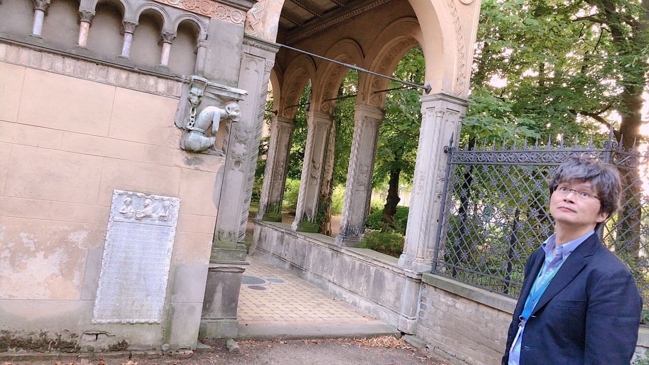
Noboru Ohtani is Professor of School of Engineering at Kwansei Gakuin University, Hyogo, Japan. He earned his Ph.D. degree in 1993 from Imperial College London, UK. Prior to joining Kwansei Gakuin University, he was with the Advanced Technology Research Laboratories, Nippon Steel Corporation from 1984 to 2008 after graduating from Tokyo Institute of Technology, Japan, where he obtained MSc degree in Physics in 1984. At Nippon Steel Corporation, he was responsible for leading several research projects on semiconductor materials and devices, particularly focusing on silicon carbide (SiC) semiconductor materials. For over 30 years, he has pioneered and made seminal contributions to the development and manufacturing of large high-quality SiC single crystals and substrates. Because of these outstanding achievements, he received the Japan Institute of Metals (JIM) Technical Development Award in 1997 and Nikkei BP Technology Award in 2008 for his prominent contribution to the development of bulk crystal growth technology of SiC single crystals. He also received a Fellow award from the Japan Society of Applied Physics (JSAP) for his seminal research contributions to SiC bulk crystal growth and defect physics in 2021. Prof. Ohtani has authored, co-authored or edited 2 books, 24 book chapters and more than 140 peer-reviewed technical papers in the field of science and technology of semiconductor materials and devices. He has served as executive and technical program committee members for a number of international conferences related to crystal growth and wide bandgap semiconductors. He is a member of JSAP, the Electrochemical Society (ECS), the Physical Society of Japan (JPS), and the Japanese Association for Crystal Growth (JACG). He currently serves as a member of the editorial bord of Applied Physics Express (APEX) and Japanese Journal of Applied Physics (JJAP) and also served as a guest editor of ECS Journal of Solid State Science and Technology: Focus Issue on “Wide Bandgap Power Semiconductors” in 2013 and of IEEE Transactions on Electron Devices: Special Issue on “Wide Band-gap Power Semiconductor Devices for Energy Efficiency and Renewable Energy Utilization” in 2014. He also serves as a co-organizer of a series of ECS symposia “GaN and SiC Power Technologies” since 2012. His current research focuses on crystal growth and defect physics in wide bandgap SiC single crystals with a view to improving the crystal quality.


